


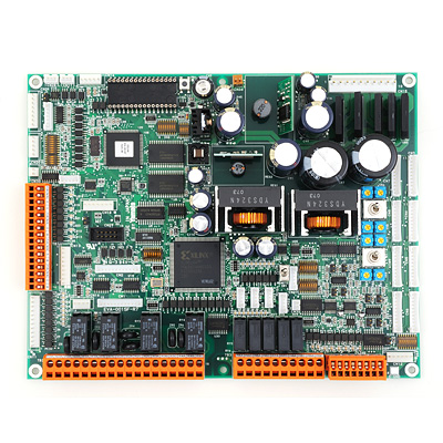
Discrete printed circuit boards
Surface-mount printed circuit boards
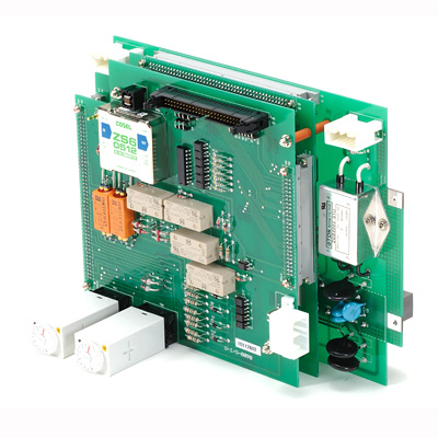
Structural printed circuit boards
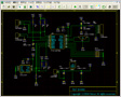 |
We manufacture a wide array of printed circuit boards, from single-sided boards to multilayer and flexible boards. Thanks to our accumulated expertise and highly reliable design capability, we are able to satisfy customer needs through services including system design, circuit design, printed circuit board design, and pattern design. |
|---|
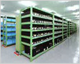 |
We deal with hundreds of major manufacturers of electronic components, allowing us to select and procure the components that best meet each application’s needs. Electronic components are stored in areas equipped with robust anti-static systems, and we have built a highly reliable environment for their handling, starting at the component inventory control stage. |
|---|
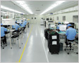 |
The printed circuit board assembly area comprises a Class 1 work environment thanks to indoor pressure control by an air conditioning system that draws on outside air. As with component storage areas, all flooring and work areas such as workbenches incorporate anti-static measures, completely eliminating component damage caused by static electricity. *Class 1 work environment: An environment in which the concentration of dust particles of 1μ㎜ or larger in size is 100,000 particles per cubic foot per minute or less. |
|---|
 |
We operate automated soldering machines on one lead-free and one leaded line, allowing us to accommodate customer specifications with a high degree of flexibility, from prototypes to mass production and design changes. |
|---|
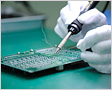 |
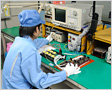
Components that cannot be soldered using automated (flow) soldering are soldered into place by hand. Additionally, flow-soldered parts are checked visually, and any defects are repaired. |
|---|
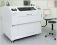 |
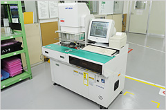
We have a high-speed flying-probe in-circuit tester (ICT) that uses mounting coordinate data to perform continuity testing of all boards. This system is particularly useful during multi-model, small-lot production runs. |
|---|
 |
We conduct a full range of electrical tests on individual boards in accordance with customer needs, allowing us to ship products of the highest quality. |
|---|
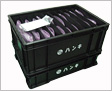 |
We package and ship products using reusable cartons with anti-static measures designed specifically for use with printed circuit boards. When shipping products directly to customers’ plants and other facilities, we package boards individually in anti-static bags. |
|---|
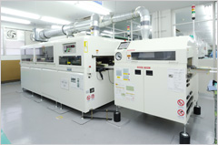
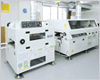
Automated soldering (flow) tank
We have one automated soldering tank each for lead-free and leaded solder processes. By analyzing and managing the solder composition of each tank once a month, we are able to achieve high-quality soldering.
Bed-of-nails in-circuit tester
This in-circuit tester (ICT) applies a bed-of-nails test fixture while the board under test is in an energized state, allowing it to test all the board’s circuits at once. Used primarily with mass-produced and high-volume lot products, it helps dramatically reduce testing man-hours.
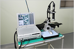
Microscope
We have a microscope to allow the installation status and solder profile for small boards and electronic components, which continue to shrink in size, to be checked visually.